- 您现在的位置:买卖IC网 > Sheet目录508 > SI3443DV (Fairchild Semiconductor)MOSFET P-CH 20V 4A SSOT-6
�� �
�
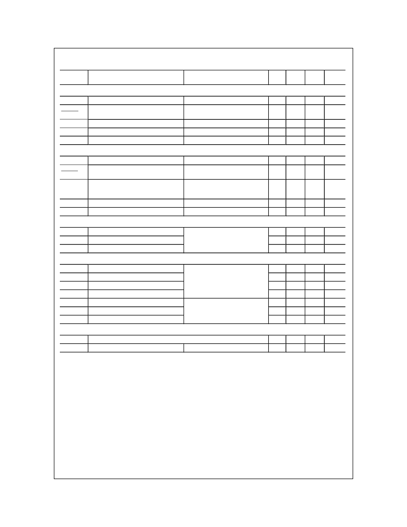
�Electrical� Characteristics�
�T� A� =� 25°C� unless� otherwise� noted�
�Symbol�
�Parameter�
�Test� Conditions�
�Min�
�Typ�
�Max� Units�
�Off� Characteristics�
�BV� DSS�
�?� BV� DSS�
�Drain-Source� Breakdown� Voltage�
�Breakdown� Voltage� Temperature�
�V� GS� =� 0� V,� I� D� =� -250� μ� A�
�I� D� =� -250� μ� A,� Referenced� to� 25� °� C�
�-20�
�-16�
�V�
�mV/� °� C�
�?� T� J�
�Coefficient�
�I� DSS�
�I� GSSF�
�I� GSSR�
�Zero� Gate� Voltage� Drain� Current�
�Gate-Body� Leakage� Current,� Forward�
�Gate-Body� Leakage� Current,� Reverse�
�V� DS� =� -16� V,� V� GS� =� 0� V�
�V� GS� =� 8� V,� V� DS� =� 0� V�
�V� GS� =� -8� V,� V� DS� =� 0� V�
�-1�
�100�
�-100�
�μ� A�
�nA�
�nA�
�On� Characteristics�
�(Note� 2)�
�V� GS(th)�
�?� V� GS(th)�
�Gate� Threshold� Voltage�
�Gate� Threshold� Voltage�
�V� DS� =� V� GS� ,� I� D� =� -250� μ� A�
�I� D� =� -250� μ� A,� Referenced� to� 25� °� C�
�-0.4�
�-0.7�
�2.5�
�-1.5�
�V�
�mV/� °� C�
�?� T� J�
�Temperature� Coefficient�
�R� DS(on)�
�Static� Drain-Source�
�On-Resistance�
�V� GS� =� -4.5� V,� I� D� =� -4� A�
�V� GS� =� -4.5� V,� I� D� =� -4� A,� T� J� =125� °� C�
�0.054�
�0.076�
�0.065�
�0.105�
�?�
�V� GS� =� -2.5� V,� I� D� =� -3.2� A�
�0.077�
�0.100�
�I� D(on)�
�g� FS�
�On-State� Drain� Current�
�Forward� Transconductance�
�V� GS� =� -4.5� V,� V� DS� =� -5� V�
�V� DS� =� -5� V,� I� D� =� -4� A�
�-10�
�9�
�A�
�S�
�Dynamic� Characteristics�
�C� iss�
�C� oss�
�C� rss�
�Input� Capacitance�
�Output� Capacitance�
�Reverse� Transfer� Capacitance�
�V� DS� =� -10� V,� V� GS� =� 0� V�
�f� =� 1.0� MHz�
�640�
�180�
�90�
�pF�
�pF�
�pF�
�Switching� Characteristics�
�(Note� 2)�
�t� d(on)�
�t� r�
�t� d(off)�
�t� f�
�Q� g�
�Q� gs�
�Q� gd�
�Turn-On� Delay� Time�
�Turn-On� Rise� Time�
�Turn-Off� Delay� Time�
�Turn-Off� Fall� Time�
�Total� Gate� Charge�
�Gate-Source� Charge�
�Gate-Drain� Charge�
�V� DD� =� -10� V,� I� D� =� -1� A�
�V� GS� =� -4.5� V,� R� GEN� =� 6� ?�
�V� DS� =� -10� V,� I� D� =� -4� A�
�V� GS� =� -4.5� V,�
�11�
�19�
�26�
�35�
�7.2�
�1.7�
�1.6�
�20�
�30�
�42�
�55�
�10�
�ns�
�ns�
�ns�
�ns�
�nC�
�nC�
�nC�
�Drain-Source� Diode� Characteristics� and� Maximum� Ratings�
�I� S�
�Maximum� Continuous� Drain-Source� Diode� Forward� Current�
�-1.3�
�A�
�V� SD�
�Drain-Source� Diode� Forward� Voltage�
�V� GS� =� 0� V,� I� S� =� -1.3� A�
�(Note� 2)�
�-0.75�
�-1.2�
�V�
�Notes:�
�1.� R� θ� JA� is� the� sum� of� the� junction-to-case� and� case-to-ambient� thermal� resistance� where� the� case� thermal� reference� is� defined� as� the� solder� mounting� surface�
�of� the� drain� pins.� R� θ� JC� is� guaranteed� by� design� while� R� θ� CA� is� determined� by� the� user's� board� design.�
�a)� 78� °� C/W� when� mounted� on� a� 1.0� in� 2� pad� of� 2� oz.� copper.�
�b)� 156� °� C/W� when� mounted� on� a� minimum� pad� of� 2� oz.copper.�
�2.� Pulse� Test:� Pulse� Width� ≤� 300� μ� s,� Duty� Cycle� ≤� 2.0%�
�Si3443DV,� REV� A�
�发布紧急采购,3分钟左右您将得到回复。
相关PDF资料
SI3445DV-T1-GE3
MOSFET P-CH 8V 6-TSOP
SI3454ADV-T1-GE3
MOSFET N-CH 30V 3.4A 6TSOP
SI3455ADV-T1-GE3
MOSFET P-CH 30V 2.7A 6TSOP
SI3457BDV-T1-GE3
MOSFET P-CH 30V 3.7A 6-TSOP
SI3457DV
MOSFET P-CH 30V 4A SSOT-6
SI3458BDV-T1-GE3
MOSFET N-CH 60V 4.1A 6-TSOP
SI3460BDV-T1-GE3
MOSFET N-CH 20V 8A 6-TSOP
SI3460DV-T1-E3
MOSFET N-CH 20V 5.1A 6TSOP
相关代理商/技术参数
SI3443DV_NL
制造商:Fairchild Semiconductor Corporation 功能描述:
SI3443DV_Q
功能描述:MOSFET SSOT6 SINGLE PCH RoHS:否 制造商:STMicroelectronics 晶体管极性:N-Channel 汲极/源极击穿电压:650 V 闸/源击穿电压:25 V 漏极连续电流:130 A 电阻汲极/源极 RDS(导通):0.014 Ohms 配置:Single 最大工作温度: 安装风格:Through Hole 封装 / 箱体:Max247 封装:Tube
SI3443DV-NF073
制造商:Vishay Siliconix 功能描述:P-CH MOSFET TSOP-6 20V 65MOHM @ 4.5V - Rail/Tube
SI3443DVPBF
制造商:INTERFET 制造商全称:INTERFET 功能描述:HEXFET Power MOSFET
SI3443DV-T1
功能描述:MOSFET 20V 4.4A 2W RoHS:否 制造商:STMicroelectronics 晶体管极性:N-Channel 汲极/源极击穿电压:650 V 闸/源击穿电压:25 V 漏极连续电流:130 A 电阻汲极/源极 RDS(导通):0.014 Ohms 配置:Single 最大工作温度: 安装风格:Through Hole 封装 / 箱体:Max247 封装:Tube
SI3443DV-T1-E3
功能描述:MOSFET 20V 4.4A 2W RoHS:否 制造商:STMicroelectronics 晶体管极性:N-Channel 汲极/源极击穿电压:650 V 闸/源击穿电压:25 V 漏极连续电流:130 A 电阻汲极/源极 RDS(导通):0.014 Ohms 配置:Single 最大工作温度: 安装风格:Through Hole 封装 / 箱体:Max247 封装:Tube
SI3443DVTR
功能描述:MOSFET P-CH 20V 4.4A 6-TSOP RoHS:否 类别:分离式半导体产品 >> FET - 单 系列:HEXFET® 标准包装:1,000 系列:MESH OVERLAY™ FET 型:MOSFET N 通道,金属氧化物 FET 特点:逻辑电平门 漏极至源极电压(Vdss):200V 电流 - 连续漏极(Id) @ 25° C:18A 开态Rds(最大)@ Id, Vgs @ 25° C:180 毫欧 @ 9A,10V Id 时的 Vgs(th)(最大):4V @ 250µA 闸电荷(Qg) @ Vgs:72nC @ 10V 输入电容 (Ciss) @ Vds:1560pF @ 25V 功率 - 最大:40W 安装类型:通孔 封装/外壳:TO-220-3 整包 供应商设备封装:TO-220FP 包装:管件
SI3443DV-TR
制造商:International Rectifier 功能描述: